| CPC H01L 29/7869 (2013.01) [H01L 27/124 (2013.01); H01L 27/1214 (2013.01); H01L 27/1225 (2013.01); H01L 27/1248 (2013.01); H01L 29/401 (2013.01); H01L 29/42384 (2013.01); H01L 29/45 (2013.01); H01L 29/4908 (2013.01)] | 7 Claims |
|
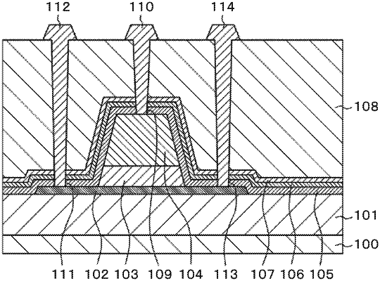
1. A TFT circuit board comprising;
a substrate;
an undercoat film formed on the substrate;
an oxide semiconductor layer formed on the undercoat film;
a gate insulating film formed on the oxide semiconductor layer; and
a gate electrode formed on the gate insulating film,
wherein
the oxide semiconductor layer includes a first semiconductor layer portion that is overlapped with the gate electrode, and a second semiconductor layer portion that is not overlapped with the gate electrode,
the gate insulating film is arranged between the gate electrode and the first semiconductor layer portion,
a first interlayer insulating film directly is in contact with the second semiconductor layer portion, and covers the second semiconductor layer portion and the gate electrode,
a first film is arranged on the first interlayer insulating film, the first film is directly in contact with the first interlayer insulating film,
the first film is more resistant against dry etching with chlorine-based gas than the first interlayer insulating film,
the first interlayer insulating film contains a silicon oxide,
a first AlO film is arranged on the first film, and the first AlO film is directly in contact with the first film,
the second semiconductor layer portion of the oxide semiconductor layer includes a drain area and a source area,
a first through-hole, which is formed in the first interlayer insulating film, the first film and the first AlO film, is connected to the drain area of the second semiconductor layer portion,
a second through-hole, which is formed in the first interlayer insulating film, the first film and the first AlO film, is connected to the source area of the second semiconductor layer portion,
a third through-hole, which is formed in the first interlayer insulating film, the first film and the first AlO film, is connected to the gate electrode over the first semiconductor portion, and
a distance between a top surface of the first AIO film covering the first semiconductor layer portion and a top surface of the first semiconductor portion is larger than another distance between the top surface of the first AIO film covering the second semiconductor layer portion and a top surface of the second semiconductor portion.
|