| CPC H01L 29/78651 (2013.01) [H01L 29/42384 (2013.01); H01L 29/785 (2013.01); H01L 2029/7858 (2013.01)] | 20 Claims |
|
1. A method for forming a semiconductor device structure, comprising:
forming a first fin structure and a second fin structure over a semiconductor substrate, wherein each of the first fin structure and the second fin structure has a plurality of sacrificial layers and a plurality of semiconductor layers laid out alternately;
forming a dielectric fin to fill a space between the first fin structure and the second fin structure;
removing the plurality of sacrificial layers to release a plurality of semiconductor nanostructures constructed by the plurality of semiconductor layers;
forming a sacrificial material on the first fin structure and the second fin structure before the dielectric fin is formed;
removing the sacrificial material and the plurality of sacrificial layers in a same etching process;
forming a metal gate stack to wrap around each of the plurality of semiconductor nanostructures;
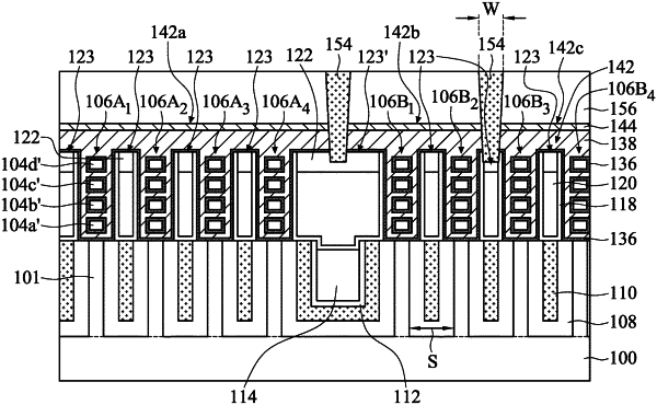
forming an insulating structure extending into the metal gate stack and reaching the dielectric fin, wherein the insulating structure and the dielectric fin together separate the metal gate stack into a first part and a second part, and the first part is electrically isolated from the second part.
|