| CPC H01L 29/785 (2013.01) [H01L 21/823821 (2013.01); H01L 29/6656 (2013.01); H01L 29/66795 (2013.01)] | 6 Claims |
|
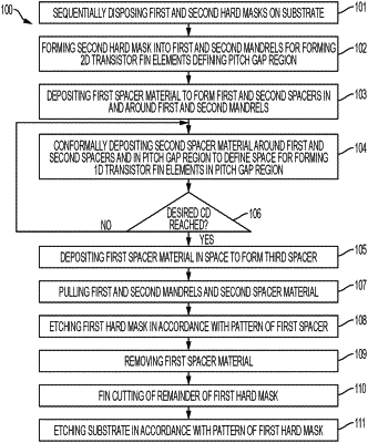
1. A method of forming a transistor structure, the method comprising:
forming on a substrate first and second mandrels for forming two-dimensional (2D) transistor fin elements defining a pitch gap region;
depositing and anisotropically etching back first spacer material to form a first spacer around the first mandrel and to form a second spacers around the second mandrel;
conformally depositing and anisotropically etching back second spacer material around the first and second spacers and in the pitch gap region to define space for forming an odd number of one-dimensional (1D) transistor fin elements in the pitch gap region; and
cyclically depositing and anisotropically etching back the first spacer material in the space to fill the space to form a third spacer,
wherein the conformally depositing of the second spacer material is executed such that a critical dimension (CD) of the space differs from a corresponding CD of the 2D transistor fin elements.
|