| CPC H01L 29/6681 (2013.01) [H01L 21/3086 (2013.01); H01L 21/76224 (2013.01); H01L 27/0886 (2013.01); H01L 29/785 (2013.01)] | 20 Claims |
|
1. A device comprising:
a fin-like field effect transistor (FinFET) device having:
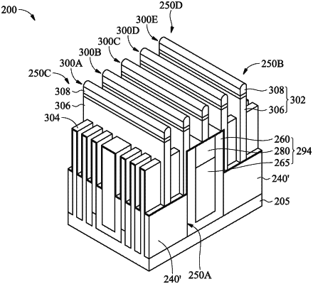
a fin structure that includes a dielectric fin and a semiconductor fin extending along a first direction, wherein the dielectric fin is disposed adjacent to the semiconductor fin, and further wherein a first width of the dielectric fin is the same as a second width of the semiconductor fin;
an isolation feature disposed between the dielectric fin and the semiconductor fin, wherein the dielectric fin includes a first dielectric material and the isolation feature includes a second dielectric material that is different than the first dielectric material; and
a gate structure disposed over a portion of the dielectric fin and a portion of the semiconductor fin, wherein the gate structure extends along a second direction that is perpendicular to the first direction.
|