| CPC H01L 27/1262 (2013.01) [H01L 27/1218 (2013.01); H01L 21/31111 (2013.01); H01L 21/31144 (2013.01)] | 10 Claims |
|
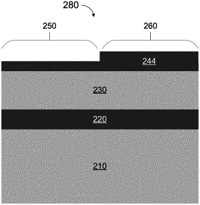
1. A method of manufacturing a barrier stack, comprising:
forming, in sequence, on a substrate comprising a metal foil and containing a diffusible element and/or species, a first barrier layer, an insulator layer, and a second barrier layer, wherein the second barrier layer has an original thickness less than the first barrier layer;
forming a blocking mask in one or more first regions of the substrate; and
thinning the second barrier layer in the one or more first regions of the substrate without thinning the second barrier layer in one or more second regions of the substrate, wherein the second barrier layer in the one or more first regions of the substrate has a final thickness that is 5 to 75% of the original thickness after thinning.
|