| CPC H01L 27/124 (2013.01) [H01L 25/167 (2013.01)] | 12 Claims |
|
1. A display panel, comprising:
a substrate;
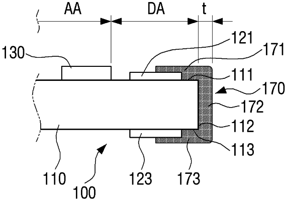
a plurality of micro light emitting diodes (LEDs) arranged on one surface of the substrate; and
a plurality of side wirings formed at an edge of the substrate to electrically connect the one surface of the substrate to an opposite surface to the one surface,
wherein each of the plurality of side wirings is connected to the one surface, a side end surface, and the opposite surface to the one surface of the substrate,
wherein both ends of each of the plurality of side wirings are electrically connected to a first connection pad and a second connection pad formed at the edge of the substrate, respectively,
wherein the first connection pad is directly disposed on the one surface of the substrate and the second connection pad is directly disposed on the opposite surface of the substrate, and
wherein both ends of each of the plurality of side wirings cover the first connection pad and the second connection pad.
|