| CPC H01L 27/0924 (2013.01) [H01L 21/823431 (2013.01); H01L 29/0649 (2013.01); H01L 29/66795 (2013.01); H01L 29/7851 (2013.01)] | 10 Claims |
|
1. A semiconductor structure, comprising:
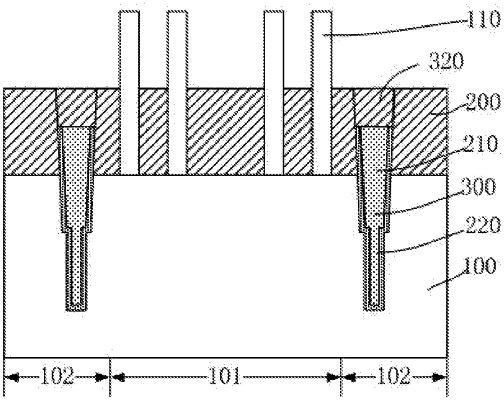
a substrate, wherein the substrate includes a first region and a second region adjacent to the first region;
a plurality of fins formed over the first region of the substrate;
an isolation layer over the substrate between adjacent fins of the plurality of fins, wherein a top of the isolation layer is lower than a top surface of a fin of the plurality of fins, the isolation layer over the second region and the second region of the substrate together contain a power rail opening, and the substrate contains a through-hole at a bottom of the power rail opening; and
a first metal layer in the power rail opening and the through-hole, wherein a back surface of the first metal layer is above a back surface of the substrate.
|