| CPC H01L 27/0922 (2013.01) [H01L 21/823842 (2013.01); H01L 29/42392 (2013.01); H01L 29/4966 (2013.01); H01L 29/517 (2013.01); H01L 29/78696 (2013.01)] | 20 Claims |
|
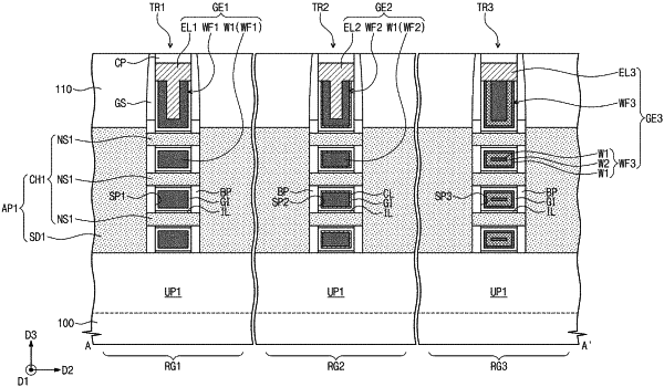
1. A semiconductor device, comprising:
a substrate including a PMOSFET region; and
a first transistor and a second transistor that are on the PMOSFET region,
wherein each of the first and second transistors includes:
a plurality of semiconductor patterns vertically stacked on the PMOSFET region and vertically spaced apart from each other; and
a gate dielectric pattern and a metal pattern filling a space between the semiconductor patterns, wherein
the gate dielectric pattern of the second transistor contains lanthanum or aluminum, and
a threshold voltage of the first transistor is different from that of the second transistor, wherein
a first length of one of the plurality of semiconductor patterns included in the first transistor is same as a second length of one of the plurality of semiconductor patterns included in the second transistor.
|