| CPC H01L 27/0886 (2013.01) [H01L 21/76898 (2013.01); H01L 21/8258 (2013.01); H01L 21/845 (2013.01); H01L 23/481 (2013.01); H01L 23/5226 (2013.01); H01L 24/29 (2013.01); H01L 24/32 (2013.01); H01L 27/0924 (2013.01); H01L 24/94 (2013.01); H01L 2224/29188 (2013.01); H01L 2224/32145 (2013.01)] | 24 Claims |
|
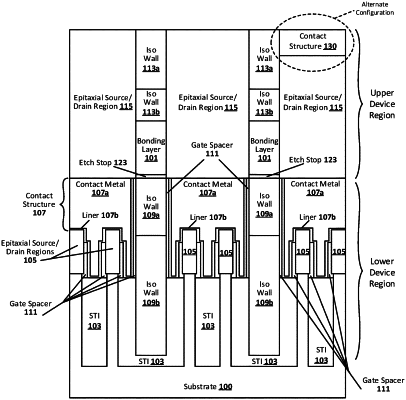
1. An integrated circuit structure, comprising:
a first transistor device layer including a first gate structure, a first source or drain region adjacent the first gate structure and comprising a first semiconductor material, and a contact structure on the first source or drain region, the first source or drain region having a lateral width along a direction; and
a second transistor device layer including a second gate structure, and a second source or drain region adjacent the second gate structure and comprising a second semiconductor material, the second source or drain region having a lateral width along the direction greater than the lateral width of the first source or drain region along the direction;
wherein the first and second transistor device layers are arranged in a vertically stacked configuration, the second semiconductor material of the second source or drain region extends downward to directly contact the contact structure on the first source or drain region, and the contact structure is vertically between the first source or drain region and the second semiconductor material of the second source or drain region.
|