| CPC H01L 27/085 (2013.01) [H01L 21/8221 (2013.01); H01L 21/823475 (2013.01); H01L 21/823481 (2013.01)] | 11 Claims |
|
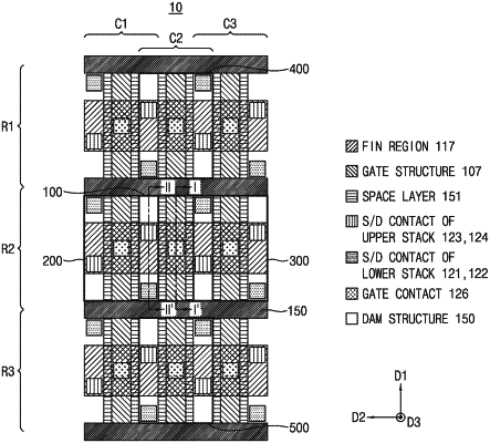
1. A method of manufacturing an array of multi-stack transistor structures, the method comprising:
providing the multi-stack transistor structures arranged in a plurality of rows and a plurality of columns in the array, each of the multi-stack transistor structures comprising a 1st transistor stack and a 2nd transistor stack formed above the 1st transistor stack;
performing gate-cut patterning along a plurality of 1st lines dividing the multi-stack transistor structures by row to form a plurality of 1st trenches;
forming a dam structure in the 1st trenches to isolate multi-stack transistor structures in one row from multi-stack transistor structures in an adjacent row in the array; and
after the forming the dam structure, forming at least a 1st source/drain contact structure landing on a 1st source/drain region of the 1st transistor stack of each of the multi-stack transistor structures.
|