US 11,742,339 B2
Light-emitting diode display panel with micro lens array
Lei Zhang, Albuquerque, NM (US); Fang Ou, Monterey Park, CA (US); and Qiming Li, Albuquerque, NM (US)
Assigned to JADE BIRD DISPLAY (SHANGHAI) LIMITED, Shanghai (CN)
Filed by Jade Bird Display (Shanghai) Limited, Shanghai (CN)
Filed on Jun. 28, 2022, as Appl. No. 17/809,405.
Application 17/133,842 is a division of application No. 16/387,896, filed on Apr. 18, 2019, granted, now 10,910,356, issued on Feb. 2, 2021.
Application 16/387,896 is a division of application No. 15/239,467, filed on Aug. 17, 2016, granted, now 10,304,811, issued on May 28, 2019.
Application 17/809,405 is a continuation of application No. 17/133,842, filed on Dec. 24, 2020, granted, now 11,417,641.
Application 15/239,467 is a continuation in part of application No. 15/007,959, filed on Jan. 27, 2016, granted, now 10,177,127, issued on Jan. 8, 2019.
Claims priority of provisional application 62/259,810, filed on Nov. 25, 2015.
Claims priority of provisional application 62/258,072, filed on Nov. 20, 2015.
Claims priority of provisional application 62/214,395, filed on Sep. 4, 2015.
Prior Publication US 2022/0336434 A1, Oct. 20, 2022
Int. Cl. H01L 25/16 (2023.01); H01L 25/075 (2006.01); H01L 25/00 (2006.01); H01L 33/52 (2010.01); H01L 23/00 (2006.01); H01L 33/58 (2010.01); H01L 33/62 (2010.01)
CPC H01L 25/167 (2013.01) [H01L 25/0753 (2013.01); H01L 25/50 (2013.01); H01L 33/52 (2013.01); H01L 24/97 (2013.01); H01L 33/58 (2013.01); H01L 33/62 (2013.01); H01L 2224/18 (2013.01); H01L 2224/73267 (2013.01); H01L 2224/92244 (2013.01); H01L 2933/0058 (2013.01); H01L 2933/0066 (2013.01)] 20 Claims
OG exemplary drawing
 
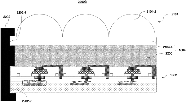
1. A light-emitting diode (LED) display panel, comprising:
a substrate;
a driver circuit array on the substrate and including a plurality of pixel driver circuits arranged in an array;
an LED array including a plurality of LED dies each being coupled to one of the pixel driver circuits;
a micro lens array including a plurality of micro lenses each corresponding to and being arranged over at least one of the LED dies;
an optical spacer formed between the LED array and the micro lens array; and
a mechanical fixture holding the driver circuit wafer and the micro lens array,
wherein the optical spacer includes an air gap.