| CPC H01L 25/0652 (2013.01) [H01L 21/4853 (2013.01); H01L 21/4857 (2013.01); H01L 21/563 (2013.01); H01L 21/565 (2013.01); H01L 21/568 (2013.01); H01L 21/6835 (2013.01); H01L 23/3128 (2013.01); H01L 23/3135 (2013.01); H01L 23/5383 (2013.01); H01L 23/5386 (2013.01); H01L 24/08 (2013.01); H01L 25/50 (2013.01); H01L 2221/68372 (2013.01); H01L 2224/08145 (2013.01); H01L 2924/18161 (2013.01)] | 20 Claims |
|
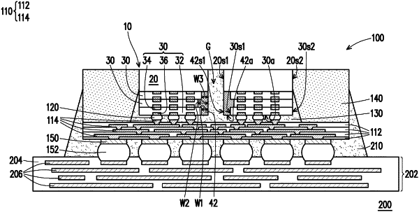
1. A semiconductor package, comprising:
a redistribution structure;
a first die and a second die between the first die and the redistribution structure, the second die electrically connected to the first die and bonded to the redistribution structure; and
a buffer layer, disposed on a first sidewall of the second die, wherein a second sidewall opposite to the first sidewall of the second die is exposed by the buffer layer.
|