US 11,742,304 B2
Radio frequency transistor amplifiers and other multi-cell transistors having isolation structures
Frank Trang, San Jose, CA (US); Qianli Mu, San Jose, CA (US); Haedong Jang, San Jose, CA (US); and Zulhazmi Mokhti, Morgan Hill, CA (US)
Assigned to Wolfspeed, Inc., Durham, NC (US)
Filed by Wolfspeed, Inc., Durham, NC (US)
Filed on Jul. 19, 2021, as Appl. No. 17/379,420.
Application 17/379,420 is a continuation of application No. 16/823,659, filed on Mar. 19, 2020, granted, now 11,069,635.
Application 16/823,659 is a continuation of application No. 16/208,940, filed on Dec. 4, 2018, granted, now 10,615,135, issued on Apr. 7, 2020.
Application 16/208,940 is a continuation in part of application No. 16/039,703, filed on Jul. 19, 2018, granted, now 10,600,746, issued on Mar. 24, 2020.
Prior Publication US 2021/0351141 A1, Nov. 11, 2021
Int. Cl. H01L 23/66 (2006.01); H01L 23/00 (2006.01); H01L 29/423 (2006.01); H01L 23/482 (2006.01)
CPC H01L 23/66 (2013.01) [H01L 23/4824 (2013.01); H01L 24/09 (2013.01); H01L 24/49 (2013.01); H01L 29/42356 (2013.01); H01L 2223/6611 (2013.01)] 20 Claims
OG exemplary drawing
 
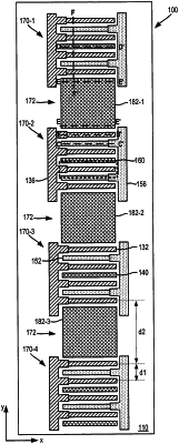
1. A transistor device, comprising:
a first unit cell transistor comprising a gate contact and a drain contact extending in a first direction;
a first electrically conductive element electrically connected to the gate contact;
a second electrically conductive element electrically connected to the drain contact;
an isolation material extending on the first unit cell transistor in a second direction that crosses the first direction, wherein the isolation material is configured to reduce a coupling between the first electrically conductive element and the second electrically conductive element; and
an isolation structure between the first unit cell transistor and a second unit cell transistor,
wherein the isolation material is electrically connected to the isolation structure.