| CPC H01L 23/544 (2013.01) [H01L 21/486 (2013.01); H01L 21/4853 (2013.01); H01L 21/4857 (2013.01); H01L 21/56 (2013.01); H01L 21/565 (2013.01); H01L 21/6835 (2013.01); H01L 21/76802 (2013.01); H01L 21/76877 (2013.01); H01L 21/78 (2013.01); H01L 23/3107 (2013.01); H01L 23/3114 (2013.01); H01L 23/3128 (2013.01); H01L 23/481 (2013.01); H01L 23/49827 (2013.01); H01L 23/5226 (2013.01); H01L 23/5383 (2013.01); H01L 23/5384 (2013.01); H01L 23/5386 (2013.01); H01L 23/5389 (2013.01); H01L 24/19 (2013.01); H01L 24/20 (2013.01); H01L 24/97 (2013.01); H01L 25/105 (2013.01); H01L 25/50 (2013.01); H01L 21/561 (2013.01); H01L 23/49816 (2013.01); H01L 24/29 (2013.01); H01L 24/32 (2013.01); H01L 24/48 (2013.01); H01L 24/73 (2013.01); H01L 24/83 (2013.01); H01L 24/92 (2013.01); H01L 25/0657 (2013.01); H01L 2221/68318 (2013.01); H01L 2221/68372 (2013.01); H01L 2221/68381 (2013.01); H01L 2223/5442 (2013.01); H01L 2223/54426 (2013.01); H01L 2223/54433 (2013.01); H01L 2223/54486 (2013.01); H01L 2224/04042 (2013.01); H01L 2224/04105 (2013.01); H01L 2224/12105 (2013.01); H01L 2224/2919 (2013.01); H01L 2224/32145 (2013.01); H01L 2224/32225 (2013.01); H01L 2224/48091 (2013.01); H01L 2224/48227 (2013.01); H01L 2224/73265 (2013.01); H01L 2224/73267 (2013.01); H01L 2224/83005 (2013.01); H01L 2224/83132 (2013.01); H01L 2224/92244 (2013.01); H01L 2224/97 (2013.01); H01L 2225/0651 (2013.01); H01L 2225/06568 (2013.01); H01L 2225/1035 (2013.01); H01L 2225/1041 (2013.01); H01L 2225/1058 (2013.01); H01L 2225/1082 (2013.01); H01L 2924/00014 (2013.01); H01L 2924/1431 (2013.01); H01L 2924/1436 (2013.01); H01L 2924/1437 (2013.01); H01L 2924/15311 (2013.01); H01L 2924/181 (2013.01)] | 20 Claims |
|
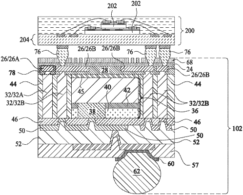
1. A method comprising:
forming a first dielectric layer;
performing a plating process to form an alignment mark over the first dielectric layer;
placing a device die over the first dielectric layer, wherein the placing is performed using the alignment mark for aligning a position of the device die;
encapsulating the alignment mark in an encapsulant;
forming a second dielectric layer over and contacting the alignment mark and the encapsulant; and
forming a plurality of redistribution lines extend into the second dielectric layer and electrically connecting to the device die, wherein the plurality of redistribution lines are formed using the alignment mark for aligning positions, and wherein at a time after the plurality of redistribution lines are formed, the alignment mark is covered by the second dielectric layer, and wherein at a time after the plurality of redistribution lines are formed, a conductive feature is formed to comprise the alignment mark and an additional redistribution line electrically connected to the alignment mark, and wherein the conductive feature is fully insulated in dielectric features.
|