| CPC H01L 23/5386 (2013.01) [H01L 21/4853 (2013.01); H01L 21/4857 (2013.01); H01L 21/563 (2013.01); H01L 21/6835 (2013.01); H01L 23/3157 (2013.01); H01L 23/5381 (2013.01); H01L 23/5383 (2013.01); H01L 24/16 (2013.01); H01L 25/0655 (2013.01); H01L 25/50 (2013.01); H01L 2221/68359 (2013.01); H01L 2224/16227 (2013.01); H01L 2924/18161 (2013.01)] | 8 Claims |
|
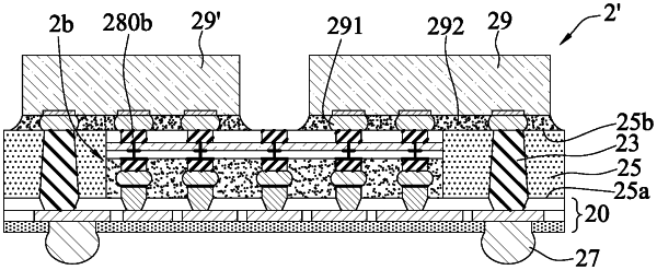
1. An electronic package, comprising:
an encapsulation layer having a first surface and a second surface opposite to each other;
a plurality of conductive pillars embedded in the encapsulation layer; and
an electronic structure embedded in the encapsulation layer and including:
an electronic body having a first side and a second side opposite to each other, and including a base and a circuit portion formed on the base, wherein the second side is defined by the base, and the first side is defined by the circuit portion, and the base includes a plurality of conductive vias electrically connected to the circuit portion and exposed from the second side;
a plurality of first conductors formed on the first side of the electronic body to electrically connect with the circuit portion;
a plurality of second conductors formed on the second side of the electronic body to electrically connect with the conductive vias;
a bonding layer formed on the first side of the electronic body to cover the first conductors, wherein the bonding layer is a film body of a non-conductive film such that side surfaces of the bonding layer are straight, and a material of the bonding layer is different from a material of the encapsulation layer;
an insulating layer formed on the second side of the electronic body to cover the second conductors;
a plurality of auxiliary conductors formed on each of the plurality of first conductors and covered by the bonding layer; and
a circuit structure formed on the first surface of the encapsulation layer and electrically connected with the plurality of conductive pillars and the electronic structure, wherein the circuit structure includes a plurality of dielectric layers and a plurality of conducive bumps are formed on the dielectric layers, such that the auxillary conductors are bonded to the conductive bumps through a surface treatment layer, and the bonding layer covers the conductive bumps.
|