| CPC H01L 23/50 (2013.01) [H01L 27/0886 (2013.01); H01L 29/785 (2013.01)] | 20 Claims |
|
1. A device structure, comprising:
a first semiconductor layer;
a second semiconductor layer on the first semiconductor layer, the second semiconductor layer being different from the first semiconductor layer in terms of composition;
a first fin and a second fin extending from the second semiconductor layer along a first direction;
a first source/drain feature disposed on the first fin;
a second source/drain feature disposed on the second fin; and
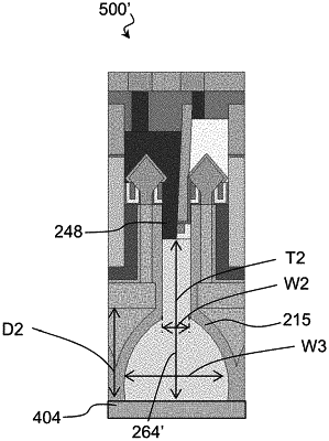
a backside metal layer extending through the first semiconductor layer and the second semiconductor layer,
wherein a portion of the backside metal layer extends above the second semiconductor layer such that the portion is disposed between the first fin and the second fin along a second direction perpendicular to the first direction,
wherein the backside metal layer is spaced apart from the first semiconductor layer, the second semiconductor layer, a sidewall of the first fin, and a sidewall of the second fin by a first dielectric layer.
|