| CPC H01L 23/49838 (2013.01) [H01L 23/49816 (2013.01)] | 19 Claims |
|
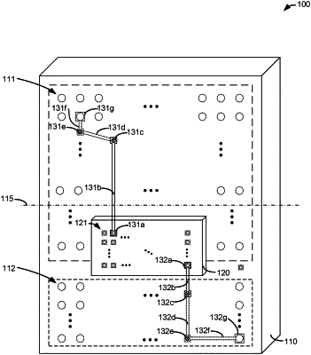
1. A packaged integrated device, comprising:
a package substrate having a first plurality of connection conductors and a second plurality of connection conductors, the first plurality of connection conductors and the second plurality of connection conductors comprising solder balls;
the package substrate having a surface that is substantially rectangular, the substantially rectangular surface having a first edge and a second edge, the first edge and the second edge defining a package centerline that is substantially parallel to the first edge and the second edge and substantially equidistant between the first edge and the second edge;
a memory buffer integrated circuit die mounted to the surface, the memory buffer integrated circuit die having a first plurality of die connections connected to the first plurality of connection conductors via a first plurality of signal conductors, the memory buffer integrated circuit die having a second plurality of die connections connected to the second plurality of connection conductors via a second plurality of signal conductors, the memory buffer integrated circuit die configured to receive at least a first plurality of command/address signals from a host via the first plurality of die connections, the memory buffer integrated circuit die configured to transmit a second plurality of command/address signals to at least one memory device via the second plurality of die connections;
the first plurality of connection conductors disposed between the package centerline and the first edge, the second plurality of connection conductors disposed between the first plurality of connection conductors and the second edge; and
the memory buffer integrated circuit die disposed such that a first average distance from the memory buffer integrated circuit die to the first plurality of connection conductors is less than a second average distance from the memory buffer integrated circuit die to the second plurality of connection conductors.
|