| CPC H01L 23/49822 (2013.01) [H01L 23/49816 (2013.01); H01L 23/49833 (2013.01); H01L 23/49838 (2013.01); H01L 24/05 (2013.01); H01L 24/16 (2013.01); H01L 25/0655 (2013.01); H01L 25/105 (2013.01); H01L 2224/0401 (2013.01); H01L 2224/05015 (2013.01); H01L 2224/05017 (2013.01); H01L 2224/05555 (2013.01); H01L 2224/05558 (2013.01); H01L 2224/05582 (2013.01); H01L 2224/16227 (2013.01); H01L 2224/16238 (2013.01); H01L 2924/1431 (2013.01); H01L 2924/1434 (2013.01); H01L 2924/182 (2013.01)] | 20 Claims |
|
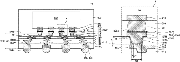
1. A semiconductor package comprising:
a redistribution substrate including a redistribution pattern;
a semiconductor chip mounted on a top surface of the redistribution substrate; and
a connection terminal between the semiconductor chip and the redistribution substrate,
wherein the redistribution substrate further comprises
a pad structure including a pad interconnection and a pad via, disposed between the redistribution pattern and the connection terminal, wherein the pad structure is electrically connected to the redistribution pattern and a top surface of the pad structure contacts the connection terminal,
a shaped insulating pattern disposed on a top surface of the redistribution pattern between the pad via and the redistribution pattern, and
a pad seed pattern disposed on the redistribution pattern and covering the shaped insulating pattern.
|