| CPC H01L 23/4275 (2013.01) [H05K 1/0203 (2013.01); H01L 24/13 (2013.01); H01L 24/16 (2013.01); H01L 2224/131 (2013.01); H01L 2224/16225 (2013.01); H01L 2924/15192 (2013.01); H01L 2924/15311 (2013.01); H01L 2924/15312 (2013.01); H01L 2924/15313 (2013.01); H01L 2924/19041 (2013.01); H01L 2924/19042 (2013.01); H01L 2924/19043 (2013.01); H01L 2924/19105 (2013.01); H05K 3/3436 (2013.01); H05K 3/4697 (2013.01)] | 19 Claims |
|
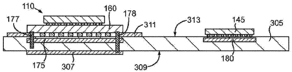
1. An apparatus, comprising:
a first semiconductor chip, a second semiconductor chip, and a circuit board, wherein:
the first semiconductor chip is mounted on and electrically coupled to the second semiconductor chip;
the second semiconductor chip is mounted on and electrically coupled to the circuit board; and
the circuit board comprises a first means for holding a phase change material and plural pins, wherein the plural pins project into the circuit board to make thermal contact with the first means for holding the phase change material and project out of the circuit board to make thermal contact with the second semiconductor chip.
|