| CPC H01L 21/823481 (2013.01) [H01L 21/76224 (2013.01); H01L 21/823487 (2013.01); H01L 27/088 (2013.01); H01L 29/6653 (2013.01); H01L 29/6656 (2013.01); H01L 29/66666 (2013.01); H01L 29/7827 (2013.01)] | 20 Claims |
|
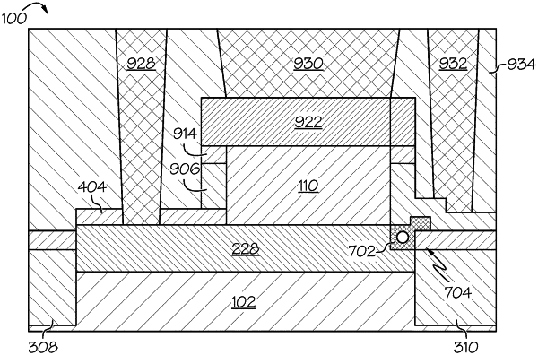
1. A method for forming a semiconductor structure comprising a plurality of vertical field effect transistors, the method comprising at least:
forming a plurality of source/drain layers each in contact with at least one semiconductor fin of a plurality of semiconductor fins and each isolated from one another by an isolation trench, wherein each isolation trench comprises an isolation material;
recessing the isolation material in each isolation trench below a top surface of the plurality of source/drain layers, wherein the recessing exposes sidewalls of the plurality of source/drain layers;
forming a spacer layer in contact with at least a top surface and the sidewalls of each source/drain layer of the plurality of source/drain layers;
removing one or more portions of the spacer layer to expose an end portion of each source/drain layer of the plurality of source/drain layers underlying a region where a gate structure is to be subsequently formed;
recessing the exposed one or more end portions, the recessing forming a notched region within each source/drain layer of the plurality of source/drain layers; and
forming a dielectric layer within each notched region.
|