| CPC H01L 21/568 (2013.01) [H01L 21/565 (2013.01); H01L 21/6835 (2013.01); H01L 21/78 (2013.01); H01L 23/3121 (2013.01); H01L 23/5383 (2013.01); H01L 23/5384 (2013.01); H01L 23/5389 (2013.01); H01L 24/00 (2013.01); H01L 24/02 (2013.01); H01L 24/19 (2013.01); H01L 24/83 (2013.01); H01L 24/97 (2013.01); H01L 25/00 (2013.01); H01L 21/561 (2013.01); H01L 24/16 (2013.01); H01L 25/0655 (2013.01); H01L 2221/68345 (2013.01); H01L 2221/68359 (2013.01); H01L 2224/02372 (2013.01); H01L 2224/02373 (2013.01); H01L 2224/04105 (2013.01); H01L 2224/12105 (2013.01); H01L 2224/16145 (2013.01); H01L 2224/16227 (2013.01); H01L 2224/16238 (2013.01); H01L 2224/18 (2013.01); H01L 2224/32225 (2013.01); H01L 2224/73267 (2013.01); H01L 2224/81005 (2013.01); H01L 2224/92244 (2013.01); H01L 2224/97 (2013.01); H01L 2924/15311 (2013.01)] | 20 Claims |
|
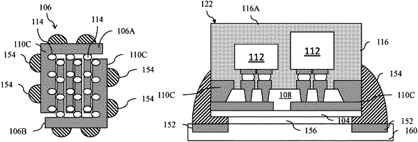
1. A semiconductor device, comprising:
a die comprising a plurality of contacts extending above a top surface of the die;
a redistribution structure directly connected to the plurality of die contacts, wherein the redistribution structure includes a routing layer width that is wider than the die;
one or more solder bumps connected to the redistribution structure, wherein the redistribution structure is between the die and the one or more solder bumps;
at least one peripheral component located laterally adjacent to the die and attached to the redistribution structure; and
an encapsulant covering the die, covering the at least one peripheral component, and surrounding the plurality of die contacts, the encapsulant extending laterally to the same width as the redistribution structure.
|