| CPC H01L 21/4853 (2013.01) [G02B 27/0927 (2013.01); H01L 24/75 (2013.01); H01L 24/81 (2013.01); H01L 23/3128 (2013.01); H01L 25/0657 (2013.01); H01L 25/50 (2013.01); H01L 2021/60112 (2013.01); H01L 2224/131 (2013.01); H01L 2224/16145 (2013.01); H01L 2224/16227 (2013.01); H01L 2224/73204 (2013.01); H01L 2224/75263 (2013.01); H01L 2224/81002 (2013.01); H01L 2224/81007 (2013.01); H01L 2224/81191 (2013.01); H01L 2224/81224 (2013.01); H01L 2224/81815 (2013.01); H01L 2224/92125 (2013.01); H01L 2225/06513 (2013.01); H01L 2924/15311 (2013.01); H01L 2924/18161 (2013.01); H01L 2924/3511 (2013.01)] | 16 Claims |
|
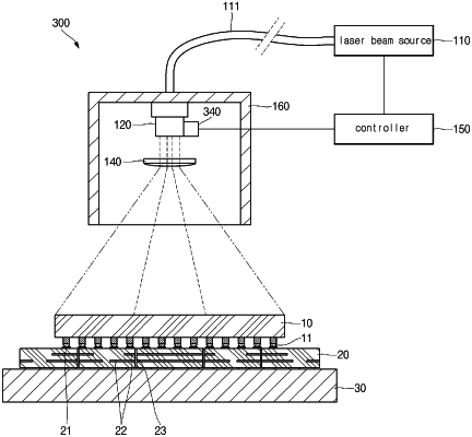
1. A method of manufacturing a semiconductor device, the method comprising:
positioning a semiconductor die on a substrate; and
irradiating the semiconductor die with a laser beam to reflow interconnection structures between the semiconductor die and the substrate,
wherein said irradiating the semiconductor die comprises:
during a first time period, laser-irradiating a first area of the semiconductor die utilizing a first amount of laser energy; and
during a second time period, laser-irradiating a second area of the semiconductor die utilizing a second amount of laser energy,
where the second area is different from the first area, and
where the second amount of laser energy is different from the first amount of laser energy.
|