| CPC H01L 21/31144 (2013.01) [H01J 37/32449 (2013.01); H01J 37/32724 (2013.01); H01L 21/0276 (2013.01); H01L 21/02274 (2013.01)] | 14 Claims |
|
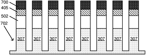
1. A method comprising:
providing a semiconductor substrate comprising a carbon-containing target layer, an anti-reflective layer, and a patterned photoresist;
patterning the anti-reflective layer to form a patterned anti-reflective mask;
exposing the semiconductor substrate to a tungsten-containing precursor and igniting a plasma under conditions to selectively deposit a tungsten-containing mask to form a patterned tungsten-containing mask on field regions of the patterned anti-reflective mask; and
patterning the carbon-containing target layer using the patterned anti-reflective mask and patterned tungsten-containing mask.
|