| CPC G11C 16/06 (2013.01) [G11C 16/0483 (2013.01)] | 10 Claims |
|
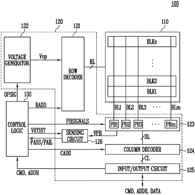
1. A memory device comprising:
a page buffer circuit including a plurality of page buffer stages each including a plurality of page buffers; and
a control circuit configured to:
generate page buffer control signals for controlling the plurality of page buffers; and
probe each of a plurality of page buffer control signal groups configured with the page buffer control signals through a probing path corresponding to each of the plurality of page buffer control signal groups,
wherein the plurality of page buffer control signal groups are configured with different kinds of page buffer control signals from each other, and
wherein the control circuit includes:
a plurality of probing pads each connected to the plurality of page buffers according to a probing control signal for turning on transistors connected between the plurality of page buffers and the plurality of probing pads, and probing any one of the plurality of page buffer control signal groups; and
a measuring pad connected to the plurality of probing pads according to a measurement control signal for turning on transistors connected between the plurality of probing pads and the measuring pad, and measuring page buffer control signal groups probed by the plurality of probing pads.
|