| CPC G11C 11/4076 (2013.01) [G11C 7/222 (2013.01); G11C 29/023 (2013.01); H03K 5/1565 (2013.01); G11C 29/028 (2013.01); H03K 5/12 (2013.01)] | 20 Claims |
|
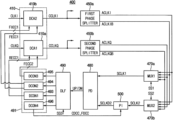
1. A quadrature error correction circuit in a semiconductor memory device, the quadrature error correction circuit comprising:
a duty cycle adjusting circuit configured to receive a first clock signal and a second clock signal which are generated based on a data clock signal, and configured to generate a first corrected clock signal and a second corrected clock signal which have a phase difference of 90 degrees with respect to each other and whose skew and duty cycle error are concurrently adjusted by adjusting a delay of a rising edge of the second clock signal with respect to a rising edge of the first clock signal, adjusting a delay of a falling edge of the first clock signal with respect to the adjusted rising edge of the second clock signal and adjusting a delay of a falling edge of the second clock signal with respect to the adjusted falling edge of the first clock signal, based on a first control code set, a second control code set, a third control code set, and a fixed control code set, the first clock signal and the second clock signal having a phase difference of 90 degrees with respect to each other;
a first phase splitter configured to split a phase of the first corrected clock signal to output a first adjusted clock signal and a third adjusted clock signal having a phase difference of 180 degrees with respect to each other;
a second phase splitter configured to split a phase of the second corrected clock signal to output a second adjusted clock signal and a fourth adjusted clock signal having a phase difference of 180 degrees with respect to each other;
a phase interpolator configured to generate a second delayed and selected clock signal by delaying a second selected clock signal having a phase difference of 90 degrees with respect to a first selected clock signal, based on a fourth control code set, the first selected clock signal and the second selected clock signal being selected from among the first through fourth adjusted clock signals;
a phase detector configured to detect a phase difference between the first selected clock signal and the second delayed and selected clock signal to generate an up/down signal; and
a delay control circuit configured to generate the first through fourth control code sets based on the up/down signal.
|