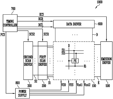
| CPC G09G 3/32 (2013.01) [G09G 2310/0278 (2013.01); G09G 2330/028 (2013.01)] | 13 Claims |

|
1. A display device comprising:
pixels;
data lines coupled to the pixels;
a first power line to supply a first initialization voltage; and
a second power line to supply a second initialization voltage,
wherein at least one of the pixels comprises:
a light emitting element having a first terminal and a second terminal;
a first transistor coupled between a first node and the first terminal of the light emitting element to control driving current of the light emitting element in response to a voltage of a second node;
a second transistor to be turned on in response to a first scan signal, the second transistor being coupled between one of the data lines and the first node;
a third transistor to be turned on in response to a second scan signal, the third transistor being coupled between the second node and a third node, and the third node being coupled between the first transistor and the light emitting element;
a fourth transistor coupled to the first node;
a fifth transistor coupled between the second node and the first power line to transfer the first initialization voltage of the first power line to the second node;
a sixth transistor coupled between the first terminal of the light emitting element and the second power line to transfer the second initialization voltage of the second power line to the first terminal of the light emitting element, and
wherein the first node is coupled to a first power source and the second terminal of the light emitting element is coupled to a second power source.
|