| CPC G06F 3/0448 (2019.05) [G02F 1/1339 (2013.01); G02F 1/13338 (2013.01); G02F 1/136286 (2013.01); G06F 2203/04107 (2013.01)] | 11 Claims |
|
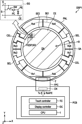
1. A display device comprising:
a first substrate;
a second substrate arranged opposite to the first substrate;
a sealant which bonds the first substrate and the second substrate and which is provided in a peripheral area surrounding a display area where an image is displayed;
a first electrode provided on the first substrate in the peripheral area;
an insulating film covering the first electrode; and
a second electrode provided on the second substrate in the peripheral area,
the sealant containing a conductive member, wherein
at least one of the first electrode and the second electrode includes a plurality of fine line portions in an area where the first electrode, the insulating film, the sealant, and the second electrode are overlapped in planar view,
the conductive member is a spherical conductive pearl, and
an interval between a first fine line portion included in the plurality of fine line portions and a second fine line portion adjacent to the first fine line portion is larger than a diameter of the conductive pearl.
|