US 11,740,744 B2
Electronic equipment
Masaki Kubo, Chiba (JP); and Shigeyuki Nishitani, Mobara (JP)
Assigned to Japan Display Inc., Tokyo (JP)
Filed by Japan Display Inc., Tokyo (JP)
Filed on Dec. 21, 2021, as Appl. No. 17/557,140.
Application 17/557,140 is a continuation of application No. 16/942,108, filed on Jul. 29, 2020, granted, now 11,237,677.
Application 16/942,108 is a continuation of application No. 16/507,515, filed on Jul. 10, 2019, granted, now 10,761,656, issued on Sep. 1, 2020.
Application 16/507,515 is a continuation of application No. 15/951,471, filed on Apr. 12, 2018, granted, now 10,394,385, issued on Aug. 27, 2019.
Application 15/951,471 is a continuation of application No. 15/270,253, filed on Sep. 20, 2016, granted, now 9,971,452, issued on May 15, 2018.
Application 15/270,253 is a continuation of application No. 15/096,396, filed on Apr. 12, 2016, granted, now 9,477,366, issued on Oct. 25, 2016.
Application 15/096,396 is a continuation of application No. 14/700,607, filed on Apr. 30, 2015, granted, now 9,335,879, issued on May 10, 2016.
Application 14/700,607 is a continuation of application No. 13/348,680, filed on Jan. 12, 2012, granted, now 9,052,757, issued on Jun. 9, 2015.
Claims priority of application No. 2011-007840 (JP), filed on Jan. 18, 2011.
Prior Publication US 2022/0113835 A1, Apr. 14, 2022
This patent is subject to a terminal disclaimer.
Int. Cl. G06F 3/044 (2006.01); G06F 3/0354 (2013.01); G06F 3/041 (2006.01)
CPC G06F 3/0443 (2019.05) [G06F 3/03547 (2013.01); G06F 3/044 (2013.01); G06F 3/0446 (2019.05); G06F 3/0412 (2013.01); G06F 3/0418 (2013.01); G06F 2203/0339 (2013.01); G06F 2203/04103 (2013.01); G06F 2203/04107 (2013.01); G06F 2203/04111 (2013.01)] 6 Claims
OG exemplary drawing
 
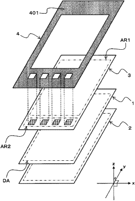
1. An electronic equipment comprising:
a first substrate;
a light shielding layer including a first opening and a second opening, on the first substrate;
a second substrate facing the first substrate;
a plurality of first detection electrodes each of which includes a plurality of first electrodes, a first connection electrode between an adjacent pair of the plurality of first electrodes, a second electrode, and a second connection electrode between an end of one of the plurality of first electrodes and the second electrode, on the second substrate; and
a plurality of second detection electrodes each of which includes a plurality of third electrodes that are located between the first electrodes,
wherein
the second connection electrode is longer than the first connection electrode,
the plurality of first electrodes overlap with the first opening,
the second electrode overlaps with the second opening, and
the second connection electrode overlaps with the light shielding layer.