| CPC G06F 1/189 (2013.01) [G06F 1/1605 (2013.01); G06F 1/1652 (2013.01); G09F 9/301 (2013.01)] | 11 Claims |
|
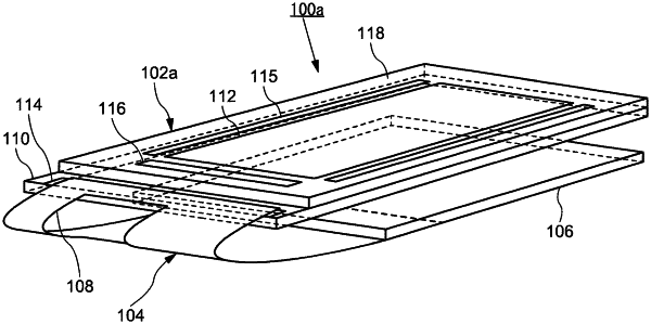
1. An electronic device, comprising:
a substrate including a first surface and a second surface opposite the first surface and including a display part including a plurality of pixels and an input terminal part on the first surface;
a wiring substrate having a flexibility connected to the input terminal part; and
an electronic component on the second surface of the substrate, wherein
the display part includes a non-display region,
the wiring substrate includes an opening through the wiring substrate,
the opening overlaps with the electronic component when the wiring substrate is bent to a side of the second surface of the substrate, and
the electronic component and the opening overlap the non-display region in the display part.
|