| CPC G03F 1/70 (2013.01) [H01L 21/0332 (2013.01); H01L 21/76895 (2013.01); H10B 12/03 (2023.02); H10B 12/482 (2023.02); H10B 12/485 (2023.02); H10B 12/488 (2023.02)] | 10 Claims |
|
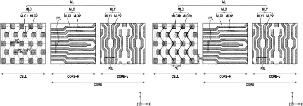
1. A method of manufacturing a photomask set, the method comprising:
preparing a mask layout, the mask layout including a plurality of first layout patterns spaced apart from one another in a first region, and distances between center points of three first layout patterns adjacent to one another from among the plurality of first layout patterns respectively have different values;
grouping pairs of first layout patterns of the plurality of first layout patterns, such that a distance between two first layout patterns adjacent to each other does not have a smallest value, and splitting the mask layout into at least two mask layout patterns; and
forming the photomask set including at least two photomasks, each photomask including a mask pattern corresponding to the first layout pattern included in each of the at least two mask layout patterns.
|