US 11,740,526 B2
Display device, method for forming a pattern and method for manufacturing display device
Seon-Il Kim, Hwaseong-si (KR); Sung Won Cho, Hwaseong-si (KR); Sang Gab Kim, Seoul (KR); Su Bin Bae, Hwaseong-si (KR); Yu-Gwang Jeong, Anyang-si (KR); and Dae Won Choi, Cheonan-si (KR)
Assigned to SAMSUNG DISPLAY CO., LTD., Yongin-si (KR)
Filed by Samsung Display Co., LTD., Yongin-si (KR)
Filed on Apr. 5, 2022, as Appl. No. 17/713,715.
Application 17/713,715 is a division of application No. 16/905,306, filed on Jun. 18, 2020, granted, now 11,320,712.
Claims priority of application No. 10-2019-0136543 (KR), filed on Oct. 30, 2019.
Prior Publication US 2022/0229322 A1, Jul. 21, 2022
Int. Cl. G02F 1/1368 (2006.01); G02F 1/1362 (2006.01); H10K 50/842 (2023.01); H10K 59/131 (2023.01); H10K 71/00 (2023.01); H10K 59/12 (2023.01)
CPC G02F 1/1368 (2013.01) [G02F 1/136286 (2013.01); H10K 50/8426 (2023.02); H10K 59/131 (2023.02); H10K 71/00 (2023.02); G02F 2202/28 (2013.01); H10K 59/1201 (2023.02)] 9 Claims
OG exemplary drawing
 
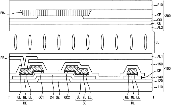
1. A display device, comprising:
a thin film transistor disposed on a base substrate; and
a signal wiring electrically connected to the thin film transistor, the signal wiring including:
a main conductive layer including copper; and
a capping layer including titanium directly on the main conductive layer, the capping layer overlapping at least a portion of an upper surface of the main conductive layer, wherein
the signal wiring has a taper angle in a range of about 70° to about 90°,
a thickness of the capping layer is in a range of about 100 Å to about 300 Å, and
a thickness of the main conductive layer is in a range of about 1,000 Å to about 20,000 Å.