| CPC G02F 1/136286 (2013.01) [G02F 1/1368 (2013.01); G02F 1/13338 (2013.01); G02F 1/13394 (2013.01); G02F 1/134363 (2013.01); G02F 1/136227 (2013.01); G06F 3/0412 (2013.01); G06F 3/0443 (2019.05); G02F 1/13396 (2021.01); G02F 1/134318 (2021.01); G02F 2201/123 (2013.01)] | 6 Claims |
|
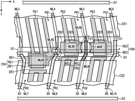
1. A display device comprising:
a plurality of pixels in a display area;
a plurality of common electrodes arranged in a matrix in the display area;
an organic insulating layer;
a first insulating layer laminated on the organic insulating layer;
a metal line between the organic insulating layer and the first insulating layer;
a second insulating layer laminated on the first insulating layer; and
an alignment film covering the second insulating layer,
wherein
the plurality of pixels have a first pixel and a second pixel adjacent to the first pixel in a first direction,
a first common electrode is one of the plurality of common electrodes,
each of the first pixel and the second pixel overlaps the first common electrode,
the first common electrode has a first slit integrally formed over the first pixel and the second pixel,
the first common electrode has a second slit formed along a boundary between the first pixel and the second pixel,
the second slit is connected to the first slit,
the first pixel has a first drain electrode of a first thin film transistor and a first pixel electrode,
the second pixel has a second drain electrode of a second thin film transistor and a second pixel electrode,
the first pixel electrode is connected to the first drain electrode at inside of the first slit,
the second pixel electrode is connected to the second drain electrode at inside of the first slit,
each of the plurality of common electrodes is separated by a third slit,
the first slit and the second slit are not connected to the third slit,
the organic insulating layer covers the first thin film transistor and the second thin film transistor,
the first common electrode is between the first insulating layer and the second insulating layer,
the first pixel electrode and the second pixel electrode are between the second insulating layer and the alignment film,
the metal line extends along the boundary of the first pixel and the second pixel,
the metal line overlaps the second slit, and
a part of the first common electrode overlaps the metal line at the boundary of the first pixel and the second pixel.
|