| CPC H10N 70/823 (2023.02) [G11C 13/0007 (2013.01); G11C 13/0011 (2013.01); H10B 63/30 (2023.02); H10N 70/021 (2023.02); H10N 70/841 (2023.02); H10N 70/883 (2023.02)] | 20 Claims |
|
1. An integrated chip including a memory device, the memory device comprising:
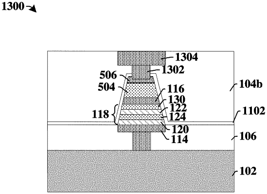
a bottom electrode disposed over a semiconductor substrate;
an upper electrode disposed over the bottom electrode, such that the bottom electrode separates the upper electrode from the semiconductor substrate;
an intercalated metal and dielectric layer stack sandwiched between the bottom electrode and the upper electrode, the intercalated metal and dielectric layer stack comprising a lower dielectric layer over the bottom electrode, an upper dielectric layer over the lower dielectric layer, and a first metal layer separating the upper dielectric layer from the lower dielectric layer; and
a chalcogenide layer over the upper dielectric layer and separating the upper dielectric layer from the upper electrode;
wherein at least one of the upper electrode and the bottom electrode have a first width and at least one of the lower dielectric layer and the upper dielectric layer have a second width that is different from the first width.
|