| CPC H10N 50/01 (2023.02) [H01F 10/3254 (2013.01); H01F 41/34 (2013.01); H10B 61/00 (2023.02); H10N 50/80 (2023.02)] | 20 Claims |
|
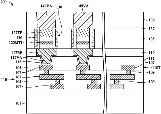
1. A magnetic random access memory (MRAM) device, comprising:
a bottom electrode over a substrate;
a magnetic tunnel junction (MTJ) structure on the bottom electrode;
a top electrode on the MTJ structure;
spacers on sidewalls of the top electrode and the MTJ structure;
a first dielectric layer surrounding the spacers;
a patterned etch stop layer on the first dielectric layer and the spacers;
a second dielectric layer on the patterned etch stop layer; and
a top electrode via embedded in the second dielectric layer and in contact with the top electrode and the patterned etch stop layer, wherein the top electrode via has a lower portion overlapping and in direct contact with a top surface and a sidewall of the patterned etch stop layer and an upper portion in direct contact with a sidewall of the second dielectric layer.
|