| CPC H10K 59/1315 (2023.02) [H10K 59/122 (2023.02); H10K 59/126 (2023.02); H01L 27/124 (2013.01); H10K 50/805 (2023.02); H10K 50/813 (2023.02); H10K 50/818 (2023.02); H10K 59/124 (2023.02); H10K 59/1213 (2023.02); H10K 59/352 (2023.02)] | 21 Claims |
|
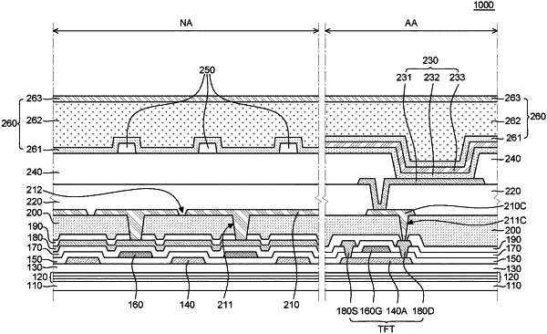
1. An electroluminescent display device comprising:
a substrate including a display area and a non-display area that is adjacent to the display area;
a transistor disposed in the display area on the substrate, the transistor including a semiconductor layer, a gate electrode, a source electrode, and a drain electrode;
a connection electrode connected to the drain electrode in the display area;
a light emitting diode disposed in the display area, the light emitting diode including a first driving electrode connected to the connection electrode, at least one light emitting layer, and a second driving electrode;
a plurality of signal lines disposed on a same layer as the semiconductor layer and the gate electrode in the non-display area;
a first intermediate layer disposed on the plurality of signal lines and the transistor;
a plurality of metal layers disposed on the plurality of signal lines, a metal layer from the plurality of metal layers disposed on a same layer as one of the source electrode and the drain electrode in the non-display area and another metal layer from the plurality of metal layers including a plurality of openings;
a second intermediate layer disposed on the metal layer, the second intermediate layer connected to the first intermediate layer though the plurality of openings in the in the non-display area; and
a protective layer disposed between the plurality of signal lines and the first intermediate layer, the protective layer including a plurality of contact holes exposing the metal layer, and
wherein the metal layer is connected to the other the metal layer though the plurality of contact holes.
|