| CPC H10K 59/131 (2023.02) [G09G 3/3233 (2013.01); G09G 2300/0426 (2013.01); G09G 2300/0439 (2013.01); G09G 2300/0819 (2013.01); G09G 2300/0842 (2013.01); G09G 2300/0861 (2013.01); G09G 2320/0242 (2013.01)] | 20 Claims |
|
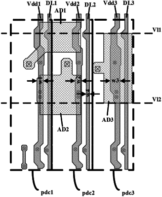
1. An array substrate, comprising:
a first data line, a second data line, and a third data line configured to provide data signals respectively to a first pixel driving circuit, a second pixel driving circuit, and a third pixel driving circuit;
a first voltage supply line, a second voltage supply line, and a third voltage supply line configured to provide a constant voltage signal respectively to the first pixel driving circuit, the second pixel driving circuit, and the third pixel driving circuit; and
a first light emitting element, a second light emitting element, and a third light emitting element respectively connected to the first pixel driving circuit, the second pixel driving circuit, and the third pixel driving circuit;
wherein a first virtual line and a second virtual line respectively cross over the first voltage supply line, the second voltage supply line, and the third voltage supply line;
the first voltage supply line, the second voltage supply line, and the third voltage supply line respectively comprise a first voltage supply line portion, a second voltage supply line portion, and a third voltage supply line portion, respectively between the first virtual line and the second virtual line;
an orthographic projection of a third anode of the third light emitting element on a base substrate completely covers an orthographic projection of the third voltage supply line portion on the base substrate; and
the third voltage supply line portion has a third line width greater than a first line width of the first voltage supply line portion, and greater than a second line width of the second voltage supply line portion.
|