| CPC H10K 59/131 (2023.02) [G09G 3/3233 (2013.01); G09G 3/3266 (2013.01); H10K 71/00 (2023.02); G09G 2300/0426 (2013.01); G09G 2300/0819 (2013.01); G09G 2300/0842 (2013.01); G09G 2300/0861 (2013.01); G09G 2310/0286 (2013.01); H10K 59/1201 (2023.02); H10K 59/1216 (2023.02)] | 19 Claims |
|
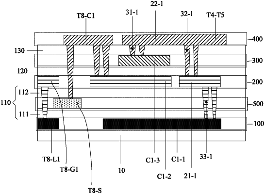
1. A display panel, comprising:
a base substrate;
a driving circuit located on the base substrate and comprising a storage capacitor;
a first conducting layer;
a second conducting layer;
a third conducting layer;
a first insulating layer located between the first conducting layer and the second conducting layer;
a second insulating layer located between the second conducting layer and the third conducting layer;
a third insulating layer located on a side, away from the base substrate, of the third conducting layer; and
a fourth conducting layer located on a side, away from the base substrate, of the third insulating layer;
wherein:
the first conducting layer, the second conducting layer and the third conducting layer are sequentially located on the base substrate in a stacked mode, and are arranged on different layers;
the first conducting layer comprises a first electrode layer, the second conducting layer comprises a second electrode layer, and the third conducting layer comprises a third electrode layer;
an orthographic projection of the first electrode layer on the base substrate, an orthographic projection of the second electrode layer on the base substrate and an orthographic projection of the third electrode layer on the base substrate have an overlap region with one another;
the first electrode layer and the third electrode layer are electrically connected with each other to serve as a first electrode of the storage capacitor, and the second electrode layer serves as a second electrode of the storage capacitor;
the second conducting layer comprises a first connecting lead insulated from the second electrode layer;
the fourth conducting layer comprises a second connecting lead; and
one end of the second connecting lead is electrically connected with the third electrode layer through first via holes penetrating through the third insulating layer, another end of the second connecting lead is electrically connected with the first connecting lead through second via holes penetrating through the second insulating layer and the third insulating layer, and the first connecting lead is electrically connected with the first electrode layer through third via holes penetrating through the first insulating layer, so that the first electrode layer is electrically connected with the third electrode layer through the first connecting lead and the second connecting lead.
|