| CPC H10K 59/1213 (2023.02) [H10K 77/10 (2023.02); H01L 27/1225 (2013.01)] | 12 Claims |
|
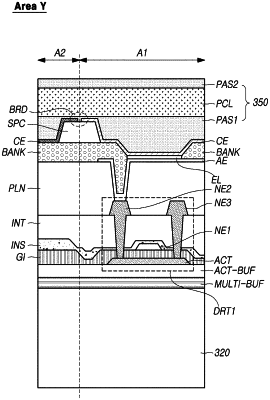
1. A display device comprising:
a substrate;
an optical device located under the substrate in a display area;
a subpixel layer located over the substrate in the display area; and
a cathode electrode layer including a cathode electrode to which a cathode voltage corresponding to a common voltage is applied,
wherein the subpixel layer includes at least one first transistor having a first characteristic and located in a first area in which the optical device is disposed, and at least one second transistor having a second characteristic and located in a second area in which the optical device is not disposed,
wherein the cathode electrode includes a first portion having a first transmittance in the first area and a second portion having a second transmittance different from the first transmittance in the second area.
|