| CPC H10B 53/30 (2023.02) [H01L 28/60 (2013.01)] | 20 Claims |
|
1. A method of forming an integrated chip, comprising:
forming an interconnect dielectric layer over a conductive structure;
forming an opening within the interconnect dielectric layer to expose a top surface of the conductive structure;
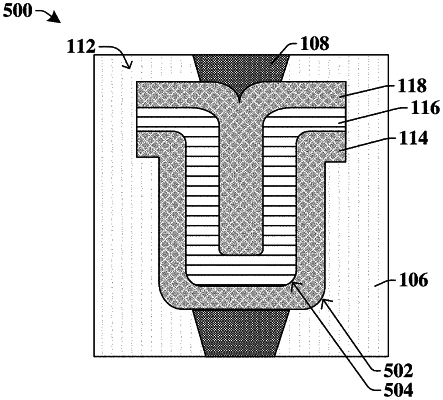
forming a first metal layer within the opening and lining outer sidewalls and a lower surface of the opening;
forming a ferroelectric layer over the first metal layer, wherein the ferroelectric layer comprises a first lower horizontal portion, a first upper horizontal portion, and a first sidewall portion coupling the first lower horizontal portion to the first upper horizontal portion;
forming a second metal layer over the ferroelectric layer;
removing peripheral portions of the first metal layer, the ferroelectric layer, and the second metal layer to form a metal-ferroelectric-metal (MFM) structure comprising the ferroelectric layer arranged between a bottom electrode and a top electrode, the ferroelectric layer having an orthorhombic phase and a non-orthorhombic phase; and
forming a second interconnect within the interconnect dielectric layer, the second interconnect having a different height than the MFM structure, wherein an imaginary horizontal line that is parallel to a top surface of the interconnect dielectric layer extends through sidewalls of both the second interconnect and the MFM structure.
|