| CPC H10B 51/20 (2023.02) [H10B 43/27 (2023.02); H10B 51/30 (2023.02)] | 20 Claims |
|
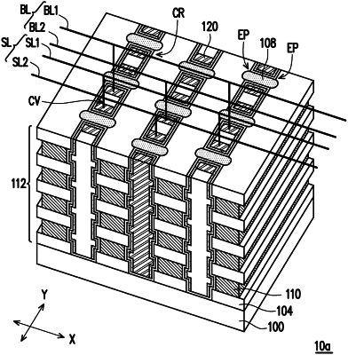
1. A three-dimensional memory device, comprising:
a first stacking structure and a second stacking structure, formed on a substrate and laterally spaced apart from each other along a lateral direction, wherein the first stacking structure comprises first insulating layers and first conductive layers alternately stacked on the substrate, and the second stacking structure comprises second insulating layers and second conductive layers alternately stacked on the substrate;
isolation pillars, extending along a vertical direction on the substrate, and extending along the lateral direction between the first stacking structure and the second stacking structure, wherein the isolation pillars laterally protrude into the first conductive layers, the first insulating layers, the second conductive layers and the second insulating layers, and a space between the first stacking structure and the second stacking structure is divided into cell regions by the isolation pillars;
gate dielectric layers, respectively formed in each of the cell regions, and covering opposing sidewalls of the first stacking structure and the second stacking structure as well as sidewalls of the isolation pillars;
channel layers, respectively covering an inner surface of one of the gate dielectric layers; and
conductive pillars, extending along the vertical direction on the substrate and located within the cell regions, wherein at least two of the conductive pillars are located in each of the cell regions and laterally surrounded by one of the channel layers, and the conductive pillars in each of the cell regions are laterally separated from one another.
|