| CPC H10B 43/30 (2023.02) [H01L 29/0649 (2013.01); H01L 29/0847 (2013.01); H10B 41/30 (2023.02)] | 20 Claims |
|
1. A method for forming an integrated chip, the method comprising:
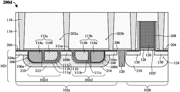
patterning a front-side surface of a substrate to define a trench extending into the front-side surface of the substrate;
performing a first ion implantation process to form a first well region in the substrate and around the trench, wherein the first well region comprises a first doping type;
depositing a gate dielectric layer over the substrate such that the gate dielectric layer lines the trench;
forming a first gate over the gate dielectric layer and within the trench such that a bottom surface of the first gate is disposed below the front-side surface of the substrate;
depositing a charge trapping dielectric structure within the trench and along the first gate;
forming a second gate over the charge trapping dielectric structure and within the trench such that the second gate is adjacent to the first gate;
forming a first source/drain region along the front-side surface of the substrate; and
forming a second source/drain region along the front-side surface of the substrate, wherein the first and second source/drain regions are disposed on opposing sides of the trench;
wherein bottom surfaces of the first and second gates are disposed vertically below a bottom surface of the first source/drain region.
|