| CPC H10B 43/27 (2023.02) [H10B 41/27 (2023.02)] | 20 Claims |
|
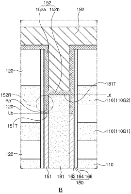
1. A method of manufacturing a three dimensional semiconductor device, the method comprising:
forming a structure including insulation layers and sacrificial layers alternately stacked on a substrate;
forming a channel hole passing through the structure;
forming a first channel structure on an inner sidewall of the channel hole;
forming a buried insulation pattern on the first channel structure in the channel hole;
recessing an upper surface of the buried insulation pattern;
removing a portion of the first channel structure, such that a top end of the first channel structure is recessed lower than the recessed upper surface of the buried insulation pattern;
forming a second channel structure on the recessed top end of the first channel structure in the channel hole; and
forming a buried conductive pattern on the second channel structure in the channel hole.
|