| CPC H10B 20/20 (2023.02) [H01L 29/0673 (2013.01); H01L 29/0847 (2013.01); H01L 29/66545 (2013.01); H01L 29/66795 (2013.01); H01L 29/785 (2013.01)] | 20 Claims |
|
1. A memory device, comprising:
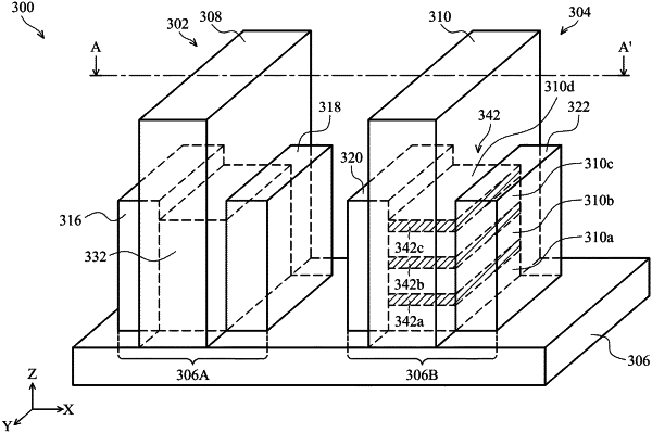
a first transistor formed in a first region of a substrate, the first transistor comprising:
a structure protruding from the substrate;
a first gate structure overlaying the protruding structure; and
a first source/drain (S/D) structure coupled to a first end of the protruding structure; and
a second transistor formed in a second region of the substrate, the second transistor comprising:
a plurality of first semiconductor layers that are vertically spaced apart from one another;
a second gate structure overlaying the plurality of first semiconductor layers, wherein the second gate structure and the first gate structure are in parallel with each other;
a second S/D structure coupled to a first end of the plurality of first semiconductor layers; and
a third S/D structure coupled to a second end of the plurality of first semiconductor layers,
wherein the first region and the second region are laterally separated from each other by an isolation structure.
|