| CPC H10B 12/37 (2023.02) [G01G 7/00 (2013.01); G01G 7/06 (2013.01); G11C 11/221 (2013.01); G11C 11/223 (2013.01); G11C 11/2275 (2013.01); G11C 19/005 (2013.01); G11C 19/18 (2013.01); H01L 28/56 (2013.01); H01L 29/516 (2013.01); H10B 12/33 (2023.02)] | 25 Claims |
|
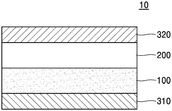
1. An electronic device comprising:
a first electrode;
a second electrode on the first electrode;
a ferroelectric film between the first electrode and the second electrode, the ferroelectric film having a first impedance; and
a dielectric film between the ferroelectric film and the second electrode, the dielectric film having a second impedance,
wherein the ferroelectric film and the dielectric film are configured to have a capacitance boosting operating voltage substantially equal to a control voltage applied between the first electrode and the second electrode, and
wherein the capacitance boosting operating voltage is determined by the following equation:
 where VMAX is the capacitance boosting operating voltage, Z1 is the first impedance, Z2 is the second impedance, tF is a thickness of the ferroelectric film, and EFM is an electric field applied to the ferroelectric film having a maximum polarization change.
|