| CPC H05K 9/00 (2013.01) [H01Q 17/007 (2013.01); H01Q 17/008 (2013.01)] | 7 Claims |
|
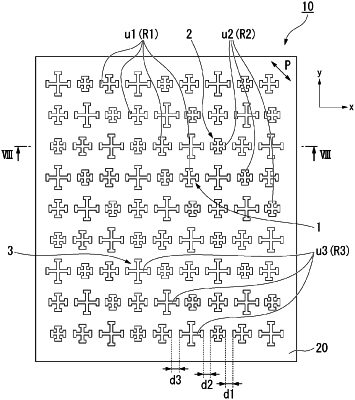
1. An electromagnetic wave absorption film comprising: a planar base; a first electromagnetic wave absorption pattern formed on the base; a second electromagnetic wave absorption pattern formed on the base; and a third electromagnetic wave absorption pattern formed on the base, wherein
when A [GHz] is defined as a frequency at which an absorption amount of an electromagnetic wave absorbed by the first electromagnetic wave absorption pattern has its local maximum value in a range from 20 to 110 GHz, B [GHz] satisfies Expression (1), B [GHz] being a frequency at which an absorption amount of an electromagnetic wave absorbed by the second electromagnetic wave absorption pattern has its local maximum value, and C [GHz] satisfies Expression (2), C [GHz] being a frequency at which an absorption amount of an electromagnetic wave absorbed by the third electromagnetic wave absorption pattern has its local maximum value,
1.037×A≤B≤1.30×A Expression (1)
0.60×A≤C≤0.963×A Expression (2).
|