| CPC H03K 5/135 (2013.01) [H03K 2005/00052 (2013.01)] | 11 Claims |
|
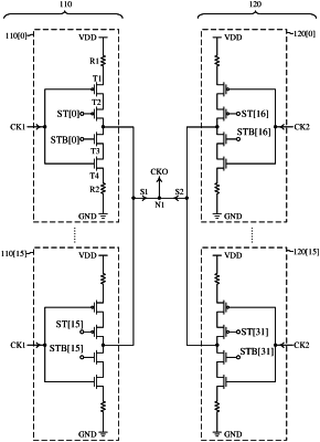
1. A phase interpolator, comprising:
a plurality of phase interpolator circuitries configured to generate an output clock signal from an output node in response to a plurality of phase control bits and a plurality of clock signals,
wherein phases of the plurality of clock signals are different from each other, each of the plurality of phase interpolator circuitries comprises a plurality of phase buffer circuits, each of the plurality of phase buffer circuits is configured to be turned on according to a first bit and a second bit in the plurality of phase control bits, in order to generate a signal component of the output clock signal to the output node according to a corresponding clock signal in the plurality of clock signals, each of the plurality of phase buffer circuits comprises a first resistor, a second resistor, and a plurality of switches and is configured to transmit one of a first voltage and a second voltage to the output node according to the corresponding clock signal, the plurality of switches are coupled between the first resistor and the second resistor, the first voltage is transmitted to the output node via the first resistor and a first group of switches in the plurality of switches, the second voltage is transmitted to the output node via the second resistor and a second group of switches in the plurality of switches, and the first resistor and the second resistor are configured to set a common mode level of the output node.
|