| CPC H03F 3/45179 (2013.01) [H03F 3/45632 (2013.01); H03F 2203/45022 (2013.01); H03F 2203/45026 (2013.01); H03F 2203/45072 (2013.01); H03K 3/35613 (2013.01)] | 20 Claims |
|
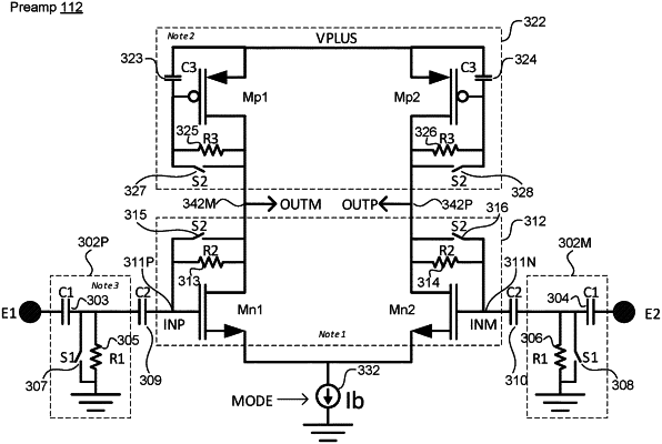
1. A fully-differential preamplifier having a differential pair of inputs including a positive input and a negative input, and a differential pair of outputs including a positive output and a negative output, the fully-differential preamplifier comprising:
first and second N-channel metal-oxide-semiconductor field-effect transistors (MOSFETs), and first and second P-channel MOSFETs, each of which includes a gate, a drain, and a source;
the sources of first and second N-channel MOSFETs connected to one another;
the sources of the first and second P-channel MOSFETs connected to one another and to a high voltage rail;
a current source connected between the connected together sources of the first and second N-channel MOSFETs and a low voltage rail;
the gate of the first N-channel MOSFET comprising the positive input of the fully-differential preamplifier;
the gate of the second N-channel MOSFET comprising the negative input of the fully-differential preamplifier;
the drains of the first N-channel MOSFET and the first P-channel MOSFET connected to one another and comprising the negative output of the fully-differential preamplifier;
the drains of the second N-channel MOSFET and the second P-channel MOSFET connected to one another and comprising the positive output of the fully-differential preamplifier;
a first resistor and a first switch connected in parallel with one another between the gate and the drain of the first N-channel MOSFET;
a second resistor and a second switch connected in parallel with one another between the gate and the drain of the second N-channel MOSFET;
a third resistor and a third switch connected in parallel with one another between the gate and the drain of the first P-channel MOSFET; and
a fourth resistor and a fourth switch connected in parallel with one another between the gate and the drain of the second P-channel MOSFET;
wherein the first, second, third and fourth switches are configured to reset an operating voltage of the fully-differential preamplifier when the first, second, third, and fourth switches are simultaneously closed for a period of time.
|