| CPC H02H 9/042 (2013.01) [G01R 19/16528 (2013.01); H02H 9/044 (2013.01); H03K 5/24 (2013.01); H03K 17/08122 (2013.01); H03K 17/6871 (2013.01); H03K 17/76 (2013.01)] | 15 Claims |
|
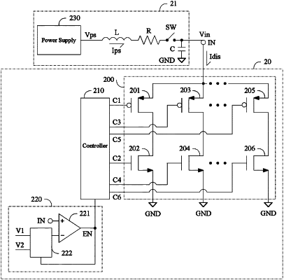
1. An overvoltage protection circuit configured to suppress a voltage spike, wherein the overvoltage protection circuit comprises:
a switch circuit, coupled directly to an input terminal with respect to the switch circuit, so as to receive an input voltage with respect to the switch circuit, wherein the switch circuit comprises a first transistor, a second transistor, a third transistor and a fourth transistor, the first transistor is coupled to the input terminal, the second transistor is coupled to the first transistor and a first terminal, the third transistor is coupled to the input terminal, and the fourth transistor is coupled to the third transistor and the first terminal;
a controller, coupled to the switch circuit for controlling the switch circuit, wherein the controller generates a first control signal, a second control signal, a third control signal, and a fourth control signal to respectively control the first transistor, the second transistor, the third transistor, and the fourth transistor; and
a comparing unit, coupled to the input terminal, wherein the comparing unit receives a first signal and a second signal, the comparing unit is configured to compare the input voltage with a first voltage and compare the input voltage with a second voltage, so as to generate an enabling signal to the controller, and the first voltage is greater than the second voltage.
|