| CPC H01S 5/0021 (2013.01) [H02J 50/12 (2016.02); H01S 5/423 (2013.01)] | 20 Claims |
|
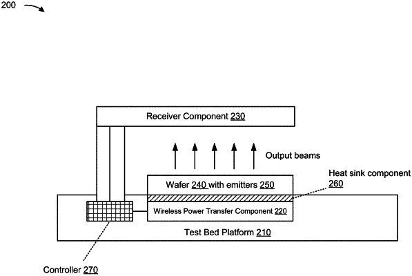
1. An electro-optical system, comprising:
a test bed configured to receive a semiconductor wafer with a set of optical emitters,
wherein an optical emitter, of the set of optical emitters, is associated with a receiver conducting medium for receiving wireless power transfer;
a wireless power transfer component configured to transfer power to the set of optical emitters of the semiconductor wafer,
wherein the wireless power transfer component is associated with a power charging conducting medium to couple to the receiver conducting medium for wireless power transfer,
wherein the power charging conducting medium and the receiver conducting medium are associated with a common resonant frequency for wireless power transfer; and
a receiver component configured to measure an optical output of the set of optical emitters.
|