| CPC H01Q 1/2283 (2013.01) [H01L 21/48 (2013.01); H01L 21/4853 (2013.01); H01L 23/498 (2013.01); H01L 23/49816 (2013.01); H01L 23/66 (2013.01); H01Q 1/22 (2013.01); H01Q 1/38 (2013.01); H01L 2223/6677 (2013.01)] | 12 Claims |
|
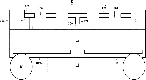
1. A semiconductor device package, comprising:
a substrate;
a first antenna comprising a first antenna pattern and a protection layer in contact with a lateral surface of the first antenna pattern;
a first support structure disposed on the substrate and configured to support the first antenna; and
a second antenna and a second support structure configured to support the second antenna, wherein the first antenna and the second antenna are disposed at different elevation,
wherein the second antenna comprises a first antenna pattern aligned with the first antenna pattern of the first antenna in a direction substantially perpendicular to the substrate, wherein the second antenna has an opening exposing a second antenna pattern of the first antenna.
|